To investigate the fundamental electronic and magnetic properties of materials, such as strongly correlated complex oxides, high quality crystals must first be fabricated to permit accurate measurement. The most advanced growth method for achieving thin films of these materials is molecular beam epitaxy (MBE), which builds crystals atomic layer by atomic layer by thermally evaporating the crystal’s constituent elements. Epitaxial growth is achieved in ultrahigh vacuum (10-10 Torr) chambers. The simplicity of MBE permits in situ, real-time analysis of crystal quality, using reflection high-energy electron diffraction (RHEED). The diffraction patterns from electrons incident upon the crystal provides information about the quality, as seen in Figure 1(a), and progression of growth. A schematic of a typical MBE system appears in Figure 1(b).
|
|
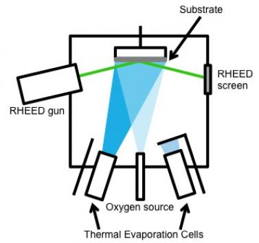 |
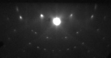
Figure 1: (a, left) RHEED pattern for a SrTiO3 substrate. (b, right) Schematic of a typical MBE chamber.
Four MBE chambers at Yale (Figure 2) permit growth of a great variety of materials. Three MBE chambers are devoted to oxide growth and one is devoted to chalcogenide growth (compounds containing Se or Te). The myriad elements currently or previously incorporated into thin films can be seen in Figure 2(e).
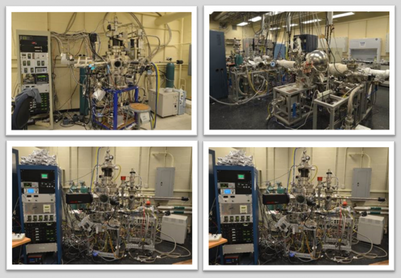
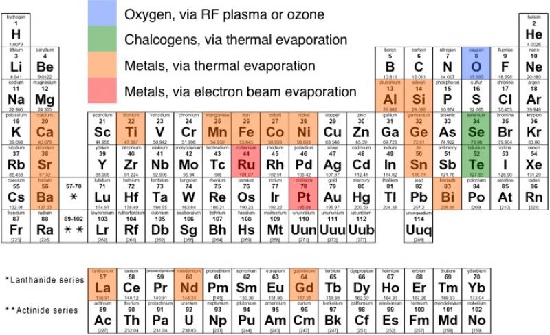
Figure 2: (a-d, top) MBE chambers at Yale available for growth of metal oxides and chalcogenides. (e, bottom) Elements currently or previously used for growth, including their growth method. (periodic table from http://www.bpc.edu)
The ultrahigh vacuum achieved in our chambers greatly reduces the occurrence of impurities and produces the highest quality thin films achievable by physical vapor deposition. The simplicity of MBE also permits the fabrication of a wide variety of heterostructures. Superlattices with atomically abrupt interfaces and thin constituent layers, such as those seen in Figure 3, are easily achievable in the MBE chambers. The high level of control in MBE also permits the growth of oxides on silicon, a crucial first step to incorporating complex oxides into Si-based field-effect transistors. Epitaxial strontium titanate (SrTiO3) on silicon appears in Figure 3(b).2
|
|
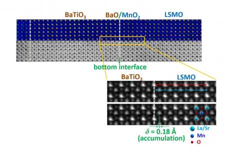
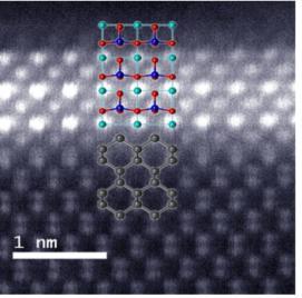
Figure 3: (a, left) Cross-sectional high-resolution TEM images of a BaTiO3/ La0.8Sr0.2TiO3 sample shows the high crystallinity achievable across interfaces.1 (b, right) High-resolution TEM shows the interface between SrTiO3 and Si.2
References
[1] Chen, H. et al. Reversible modulation of orbital occupations via an interface-induced polar state in metallic manganites. Nano Letters 14, 4965-4970, doi:10.1021/nl501209p (2014)
[2] Kolpak, A. M. et al. Interface-Induced Polarization and Inhibition of Ferroelectricity in Epitaxial SrTiO3/Si. Physical Review Letters 105 217601, doi:10.1103/PhysRevLett.105.217601 (2010).