Thin film perovskite oxides (chemical formula ABO3) present a rich and diverse set of phenomena[1-3]. One major challenge for mainstream applications of these diverse properties is integration with single crystal silicon. We have developed a number of processes for growing these oxides on diverse semiconductors, including gallium arsenide, silicon, and germanium. The key challenge to this approach is maintaining an atomically sharp interface of the semiconductor with the oxide template (Figure 1 [4]). From this template, we can deposit other compatible oxides of interest, and integrate the rich properties of complex oxides with the high mobility and widely established platform of Si (Figure 2 [5]).
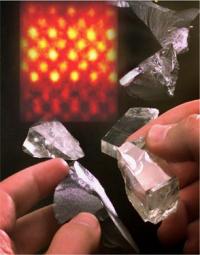 Figure 1 [4] – Photograph of a piece of silicon (left) and a large single crystal of MgO (right). This photograph represents the overall vision of integrating the properties of dramatically different materials. Inset: A transmission electron microscopy image of a cross section of a thin film of SrTiO3 grown on silicon. This image demonstrates an atomically abrupt interface, where the Sr layer in SrTiO3 makes a transition to the atoms of the silicon substrate within one atomic layer.
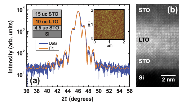
Figure 2 [5] – Heterostructures are composed of multiple oxide layers to realize new properties. Here two insulators, LaTiO3 (LTO) and SrTiO3 (STO), are combined on silicon, resulting in an oxide that conducts electricity. (a) X-ray diffraction from this oxide heterostructure, where the intensity and location of the observed peaks are sensitive to the thicknesses of each layer. Left inset: Schematic showing the layer thicknesses. Right inset: Atomic force microscopy gives a topographic map of the film surface. (b) TEM micrograph of the oxide heterostructure integrated with silicon.
References
[1] C. H. Ahn et al., Science 284, 1152 (1999)
[2] Y. H. Chu et al., Nat. Mater. 7, 478 (2008)
[3] A. Ohtomo and H. Y. Hwang, Nature 427, 423 (2004)
[4] R. A. McKee, F. J. Walker, and M. F. Chisholm, Phys. Rev. Lett. 81, 3014 (1998)
[5] E. N. Jin, et al., APL Mat. 2, 116109 (2014)